PWM (pulse width modulation) is a technology that uses pulses to output analog signals. It modulates the width of a series of pulses to produce equivalent target waveforms. It is widely used in measurement, communication, switching power supply, motor control and other fields. This article will share the basic control principles of PWM technology and common circuit applications.
Basic PWM control principle
1. Theoretical basis
Area equivalence principle: When narrow pulses with equal impulses but different shapes act on a link with inertia, their effects are basically the same. Among them, "impulse" refers to the area of the narrow pulse, and "basically the same effect" means that the output response waveform of the link is basically the same.

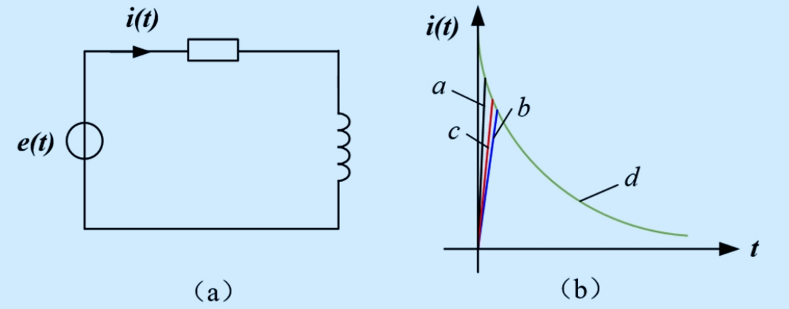
The narrow voltage pulses shown in the figure are applied to the first-order inertia link (Figure (a) below), and the output current i(t) response waveforms of each narrow pulse are shown in Figure (b) below.

It can be seen that in the initial transient state, their response waveforms are slightly different, but the subsequent response waveforms are exactly the same. The narrower the applied pulse, the smaller the difference in the waveform of the output response. If the above pulses are applied periodically, the response is also periodic. After decomposing the response signal using Fourier series, it can be seen that the characteristics of the response in the low frequency band will be very close, and only differ in the high frequency band.
2. Control principle
Based on the area equivalence principle, PWM modulates a series of pulse widths to generate a narrow pulse waveform with the same pulse impulse as the target waveform, thereby achieving the equivalence of the target waveform (including shape and amplitude).
Here, the modulation process is introduced by taking the commonly used sine half-wave equivalence as an example:

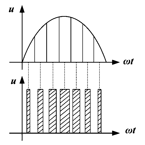
First, the sine half-wave is evenly divided into N connected pulses with equal widths and different amplitudes. Then, it is replaced by N rectangular pulses of equal amplitude and unequal width. The midpoint of the rectangular pulse coincides with the midpoint of the corresponding sine wave pulse, and the area (impulse) of the two are equal. In this way, a series of PWM waveforms equivalent to the sine half wave can be obtained - SPWM waveforms, and the pulse width of the SPWM waveform changes according to the sine law. In addition to sine waves, PWM technology can also be equivalent to DC and non-sinusoidal AC waveforms. Its basic principle is the same as SPWM control, both of which are based on the area equivalence principle.
Application of PWM Technology
PWM chopper circuit and PWM inverter circuit are the two most typical circuit applications of PWM technology. At present, most of the inverter circuits in actual application are PWM type, and PWM chopper circuit has been widely used in DC motor speed regulation. In addition, the chopping AC voltage regulation circuit and matrix frequency conversion circuit based on PWM technology are both used in the field of AC-AC conversion.
The following introduces typical DC chopper circuits and PWM inverter circuits.
1. DC chopper circuit
Commonly used DC chopper circuits include: Buck circuit, Boost circuit, Buck-Boost circuit, Cuk chopper circuit and Sepic chopper circuit.
Here we take the Buck DC chopper circuit as an example to explain, and the circuit structure is shown in the figure below:

In the figure: V is a fully controlled device, and D is a freewheeling diode.
When the device is in the on state, the power supply supplies power to the load and charges the capacitor, and the diode voltage VD=Vin; when the device is in the off state, the capacitor supplies power to the load, and the diode voltage is approximately 0.
If the switch device is periodically turned on and off, the output voltage waveform is shown in the figure on the right. The power supply is turned on during the on time ton and cut off during the off time T-ton, so it is also called chopping.
The average value of the output voltage is:

It can be seen that the DC chopper circuit can adjust the output voltage average value by adjusting the on and off time of the switching device to obtain the required DC voltage waveform.
2. PWM inverter circuit
There are two commonly used PWM inverter circuit control methods: calculation method and modulation method. Among them, the calculation method is cumbersome and needs to be recalculated when the output sine waveform changes, so the modulation method is often used to control the PWM inverter circuit. The following explains the SPWM modulation process of the single-phase bridge inverter circuit and the SVPWM modulation process of the three-phase bridge inverter circuit.
Single-phase bridge inverter circuit
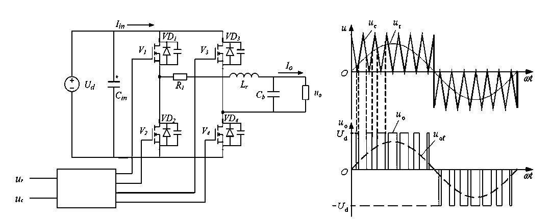
The desired output signal is used as the modulation signal, and the isosceles triangle wave or sawtooth wave is used as the carrier signal. The intersection of the two signals is used to control the on and off of the switching device, and a series of PWM pulses with a width proportional to the signal wave amplitude will be obtained.
The specific modulation process is as follows:

During the positive half cycle of the modulation signal ur: the switch device V1 remains on, V2 and V3 remain off, and V4 is turned on alternately according to the relationship between the modulation wave and the carrier.
When |Ur|>|Uc|, V4 is turned on, and the load voltage Uo=Ud; when |Ur|<|Uc|, V4 is turned off, and the load current will continue to flow through the diode D3, and the load voltage Uo=0 at this time. The output voltage Uo is a waveform that alternates between 0 and Ud levels.
In the negative half cycle of the modulation signal ur: the switch device V2 remains on, V1 and V4 remain off, and V3 is turned on alternately according to the relationship between the modulation wave and the carrier. When |Ur|>|Uc|, V3 is turned on, and the load voltage Uo=-Ud; when |Ur|<|Uc|, V3 is turned off, and D4 continues to flow, and the load voltage Uo=0 at this time. The output voltage Uo is a waveform that alternates between 0 and -Ud levels.
In one full cycle of the modulation signal wave ur, the PWM waveform output by the inverter consists of three levels: ±Ud and 0.
Three-phase bridge inverter circuit
In addition to the above-mentioned SPWM sinusoidal pulse width modulation technology, SVPWM space vector pulse width modulation technology is also very commonly used in the field of motor control.
SPWM is to generate a rotating magnetic motive force in space by passing a sine wave with a phase difference of 120° into the motor stator to drive the rotor to rotate. SVPWM, on the other hand, forms a rotating voltage vector in the motor by setting the on and off of the switch tube, thereby generating a rotating magnetic motive force.
The specific implementation method of SVPWM is as follows:
The circuit is composed of six switching devices, and the upper and lower tubes are a group to form three half-bridge circuits.
The upper and lower bridge arms of the same half bridge cannot be turned on or off at the same time. Define the state as 1 when the upper bridge arm is turned on and the lower bridge arm is turned off, and the state as 0 when the upper bridge arm is turned off and the lower bridge arm is turned on, then 8 voltage states can be obtained (000, 100, 110, 010, 011, 001, 101, 111). Among them, 000 and 111 are zero vectors, and the other six are non-zero voltage vectors, dividing the spatial voltage vector diagram into 6 sectors.
In the implementation process of SVPWM: First, determine the required Uα and Uβ values according to the position of the rotor and the collected current data, and then determine the sector where the voltage U synthesized by Uα and Uβ is located.
Then, select the voltage vector (U1~U6) required for the synthesized voltage U according to the determined sector, and calculate the holding time of the switching device based on the relationship of vector synthesis. Finally, control the on and off of the switching device according to these calculation results to achieve the expected voltage U output.


