Over the years, switch-mode power converters have found widespread use in modern electronics across multiple sectors including industrial, commercial, utility, and consumer markets. For low-power DC-DC conversion based applications, most modern power conversion is accomplished using three main types of power converters – buck, boost, and buck-boost. However, some specific electronic circuits require a power supply with a negative voltage on the output side. An inverting switching converter is a type of DC-DC converter that can supply a negative voltage. Most of the basic DC-DC converter topologies can be modified to be inverting converters.

The main purpose of an inverting converter is to provide a negative voltage at the output. In addition to this feature, the polarity inverting topology is very useful for power loads that are polarity independent with respect to the system ground, but are supplied by an input voltage that may be higher or lower than the output voltage. The inverting topology typically uses a single inductor and does not require any coupling capacitors. This results in fewer components being used to implement the inverting topology. However, due to the narrow range of applications it caters to, it is used less frequently than other basic DC/DC converter topologies. For scenarios that handle larger rectifier currents, synchronous buck or synchronous boost devices are employed. This helps improve efficiency by reducing conduction losses.
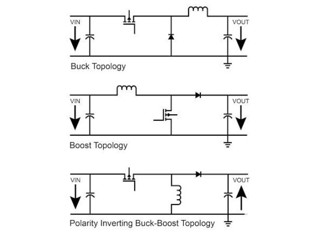
The implementation of an inverting converter can be done in many ways. It could be through a negative reference, i.e. using any buck device to convert a positive voltage to a negative voltage. It could also be through a positive reference, using any boost device to convert a negative voltage to a positive voltage. One of the specific types of inverting converter topologies is the inverting buck-boost converter. Figure 1 shows the buck topology, boost topology, and polarity inverting buck-boost topology. It is known to be a simple and low-cost polarity inverting converter with few power stage components. It has the advantages of low component count and low development complexity, and its implementation can be done using standard high-side regulator integrated chips. These are also used for buck converters.
Circuit diagram of buck topology, boost topology, and polarity inverting buck-boost switching converter. Image attributes
It is known to reverse the direction of the input voltage by utilizing a true flyback topology, and is similar to the conventional flyback converter topology as it has a 1:1 winding ratio. The current is pulsed at both the input and output. Since the output voltage flies back to the switch node, known as the flyback voltage, the voltage stress across the semiconductor-based switch is the sum of the input and output voltages. The controller is referenced to either the negative input or the negative output; therefore, it must withstand the sum of the input and output voltages.
Advanced Buck-Boost Converter Operation
The polarity inverting buck-boost converter is a basic power conversion topology. It is implemented using an active switch (usually a MOSFET), a passive switch (usually a diode), and an inductor.

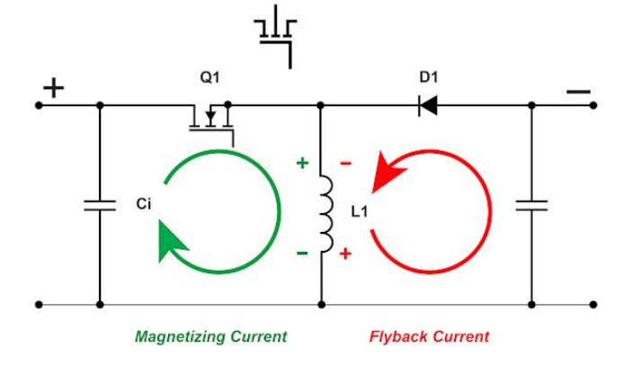
Figure 2 shows the operation of an inverting buck-boost converter. When the switch is on (called the on-time), the input voltage across the inductor forces current to ground. In this case, energy is stored in the air gap. When the diode conducts, the switch is off (called the off-time), and the inductor voltage flips and causes the rectifier to conduct. This results in a negative voltage at the output. The current flowing during the on-time is often called the magnetizing current, while the current flowing during the off-time is called the flyback current. The energy stored in the inductor during the on-time is used to drive the flyback current.


