Introduction
Electromagnetic interference (EMI) is one of the most common reasons why switching power supplies, DC/DC converters, battery chargers, and inverters fail EMC compliance testing. While modern power semiconductors such as MOSFETs, IGBTs, SiC, and GaN devices improve efficiency, their high dv/dt and di/dt characteristics significantly increase EMI challenges.
At IDEALPLUSING, we frequently encounter EMI issues in high-power DC/DC converters and battery charger projects. In one 5kW charger project, conducted EMI at approximately 500kHz exceeded CISPR 32 Class A limits by nearly 8dB. After optimizing the common-mode choke and Y-capacitor network, the product successfully passed compliance testing.
This article summarizes seven practical EMI reduction techniques based on real engineering experience.
1. Identify EMI Sources Before Fixing EMI
Common EMI sources include switching nodes, transformer leakage inductance, rectifier reverse recovery current, PCB current loops, gate-drive circuits, and long cable harnesses.
EMI is generally divided into Conducted EMI (150kHz–30MHz), Radiated EMI (>30MHz), Common-Mode Noise, and Differential-Mode Noise. Understanding the dominant noise path is the first step toward successful troubleshooting.
2. Minimize High di/dt Current Loops
Reducing loop area is one of the fastest ways to lower radiated EMI.
Engineering Example:
• Original loop area: approximately 25cm²
• Optimized loop area: approximately 8cm²
• Measured radiated EMI reduction: 6–10dB
Best practices:
• Place input capacitors close to switching devices
• Use wide copper traces and solid ground planes
• Avoid unnecessary vias in high-current paths
• Use multilayer PCB structures
3. Optimize Gate Drive Switching Speed
Many engineers pursue maximum switching speed to improve efficiency. However, excessive switching speed often increases EMI and ringing.
Engineering Example:
• Gate resistor changed from 4.7Ω to 15Ω
• Peak ringing reduced by approximately 35%
• Conducted EMI improved significantly without major efficiency loss
Recommended gate resistor ranges:
MOSFET: 5–20Ω
IGBT: 10–47Ω
GaN FET: 1–10Ω
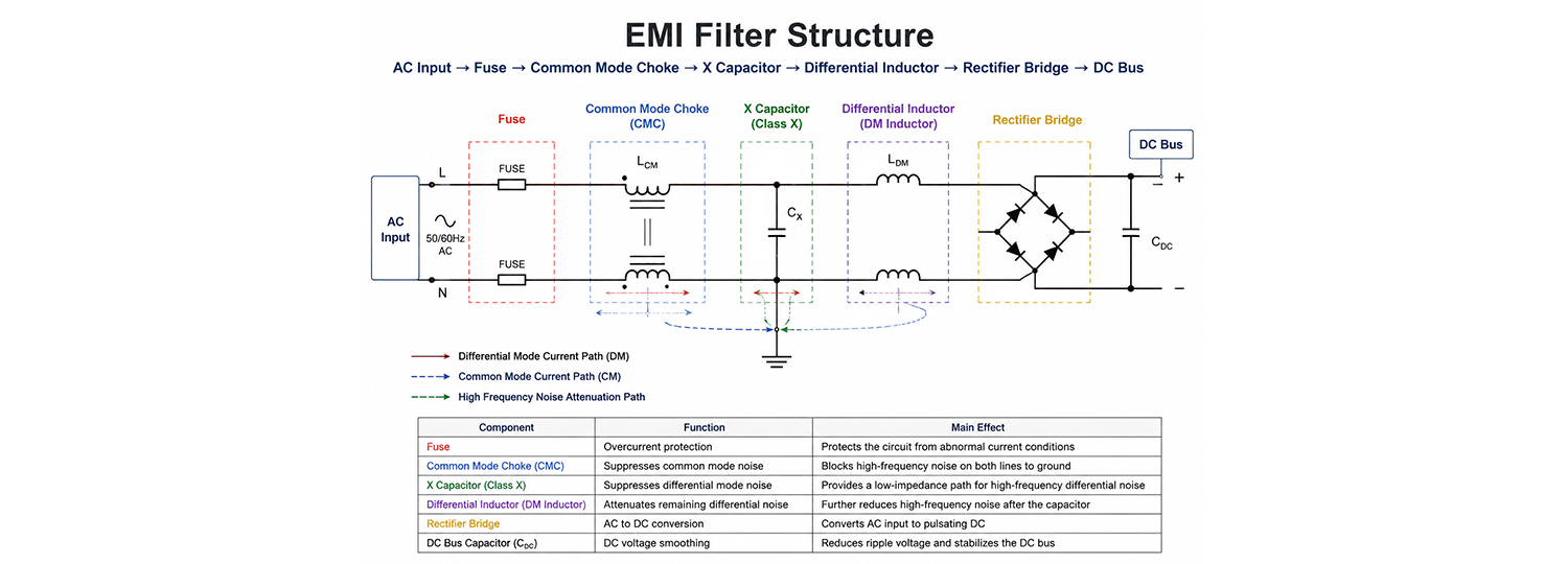
4. Design EMI Filters Correctly
A properly designed EMI filter can reduce conducted EMI by 20–40dB.
Typical filter structure:
AC Input → Fuse → Common Mode Choke → X Capacitor → Differential Inductor → Rectifier Bridge → DC Bus
Case Study:
In a recent battery charger project, increasing common-mode choke inductance from 2mH to 5mH and adding an extra Y capacitor enabled the system to pass CISPR 32 testing after previously failing by 8dB.
Keywords: EMI Filter Design, EMC Compliance, Conducted EMI, Low EMI Power Supply.
5. Improve Transformer Design
Poor transformer design is often the dominant source of common-mode noise.
Recommended methods:
• Reduce leakage inductance
• Use interleaved windings
• Add electrostatic shield layers
• Minimize parasitic capacitance
A shield winding connected to PE can significantly reduce common-mode current and improve EMC performance.
6. Optimize Grounding and Shielding
Grounding strategy directly affects EMI performance.
Best practices:
• Separate power ground and signal ground
• Use single-point grounding
• Minimize ground impedance
• Shield sensitive control circuits
• Properly ground metal enclosures above 1kW
Well-designed grounding often reduces troubleshooting time and improves overall system reliability.
7. Use Snubber Circuits to Suppress Ringing
Transformer leakage inductance and switching transitions often create high-frequency ringing.
Common options:
• RC Snubber
• RCD Snubber
• TVS Diode
• Active Clamp
Practical results:
Proper snubber tuning can reduce ringing amplitude by more than 50%, improving both EMI and long-term reliability.
EMC Compliance Checklist
• Check conducted EMI against CISPR 32 limits
• Verify common-mode current paths
• Reduce switching loop area
• Optimize gate resistor values
• Validate EMI filter design
• Inspect transformer leakage inductance
• Verify grounding and shielding strategy
• Measure ringing with an oscilloscope
• Re-test after every design modification
Conclusion
Successful EMI reduction requires a system-level approach rather than relying on a single filter component. By optimizing PCB layout, switching loops, gate drive circuits, transformer design, grounding, shielding, and EMI filters, engineers can significantly improve EMC compliance and product reliability.
For modern SiC and GaN-based power supplies, EMI considerations should be incorporated from the first day of development. This approach reduces redesign cycles, lowers certification costs, and accelerates product launch schedules.